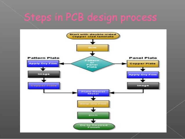
PCB Package Configurator: Simplify Your PCB Design Process! How to use a modular approach to simplify your pcb design process
If you are looking for A detailed guide to PCB layout design - IBE Electronics you've came to the right web. We have 25 Pictures about A detailed guide to PCB layout design - IBE Electronics like How to Use a Modular Approach to Simplify Your PCB Design Process, PCBWay's KiCad Plugin: Simplify Your PCB Design Process - Semiconductor and also Basic Steps to Design a PCB Layout – PCB HERO. Read more:
A Detailed Guide To PCB Layout Design - IBE Electronics
 www.pcbaaa.com
A detailed guide to PCB layout design - IBE Electronics
How To Use A Modular Approach To Simplify Your PCB Design Process
 www.linkedin.com
How to Use a Modular Approach to Simplify Your PCB Design Process
The Processes Of PCB Design That You Should Know
 how2electronics.com
The processes of PCB Design that you should know
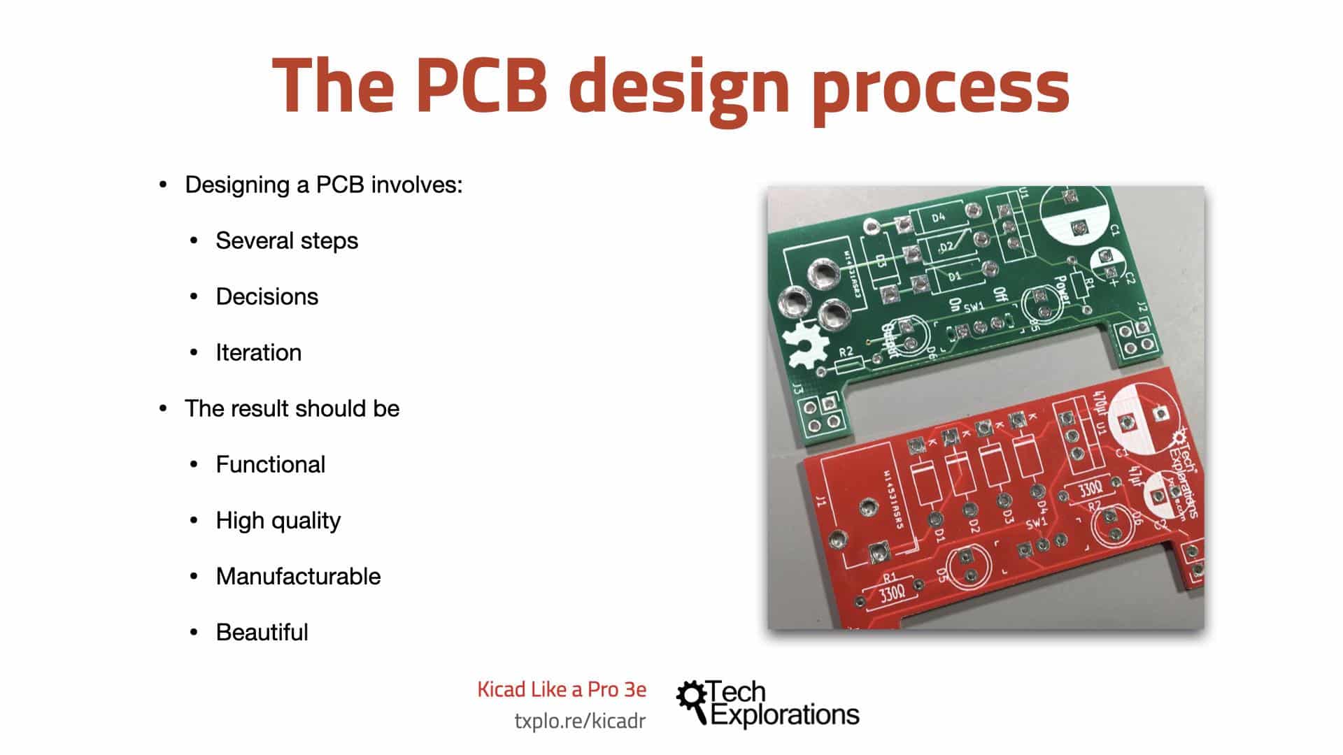
Tech Explorations - KiCad 6 Guide Series - The PCB Design Process
 techexplorations.com
Tech Explorations - KiCad 6 Guide Series - The PCB design process
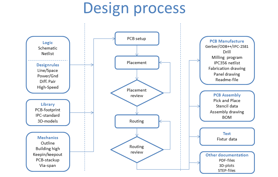
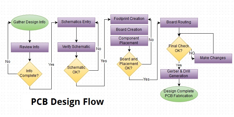
PCB Design Process
 mungfali.com
PCB Design Process
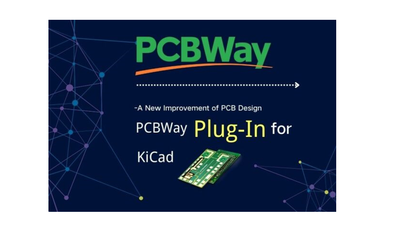
New Electronics - PCBWay's KiCad Plugin: Simplify Your PCB Design Process
 www.newelectronics.co.uk
New Electronics - PCBWay's KiCad plugin: Simplify your PCB design process
The PCB Design Process Explained -Wonderful PCB Shenzhen
 support.wonderfulpcb.com
The PCB Design Process Explained -Wonderful PCB Shenzhen
7 Steps Guide In PCB Design Process Update 2022
 gespcb.com
7 Steps Guide in PCB Design Process Update 2022
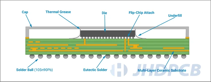
IC PCB Package Type: Importance And Guidelines - Jhdpcb
 jhdpcb.com
IC PCB Package Type: Importance And Guidelines - Jhdpcb
How To Design A PCB Board. PCB Design Process Steps Guide Of 2023
 jamindopcba.com
How to Design A PCB Board. PCB Design Process Steps Guide of 2023
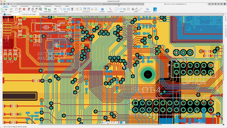
PCB Design Software | Circuit Board Design | Autodesk
 www.autodesk.com
PCB Design Software | Circuit Board Design | Autodesk
PCB Process Flow Chart | Www.homillux.com
 www.homillux.com
PCB Process Flow Chart | www.homillux.com
A Guide To Pcb Design Process Aipcba - Vrogue.co
 www.vrogue.co
A Guide To Pcb Design Process Aipcba - vrogue.co
Printed Circuit Board Design Process | Steps To Design PCB
 www.electronicsandyou.com
Printed Circuit Board Design Process | Steps to Design PCB
PCB Design Process
 mungfali.com
PCB Design Process
PCBWay's KiCad Plugin: Simplify Your PCB Design Process - Semiconductor
 www.semiconductorforu.com
PCBWay's KiCad Plugin: Simplify Your PCB Design Process - Semiconductor ...
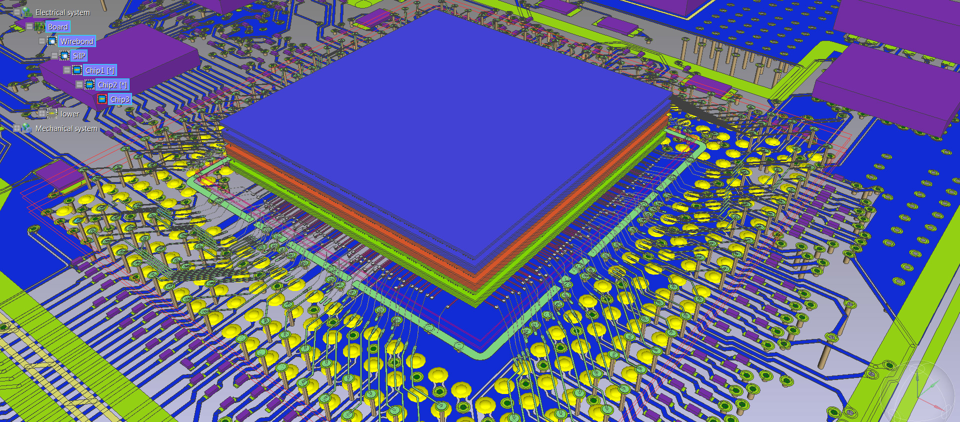
3D Convergence Of Multi-board PCB And IC Packaging Design - Zuken EN
 www.zuken.com
3D Convergence of Multi-board PCB and IC Packaging Design - Zuken EN
PCB Layout Design Process And Guidelines - ELEPCB
 www.elepcb.com
PCB Layout Design Process and Guidelines - ELEPCB
Design A Pcb Board - Draw. Imagine. Create.
 drawspaces.com
Design A Pcb Board - Draw. Imagine. Create.
PCB
 www.slideshare.net
PCB
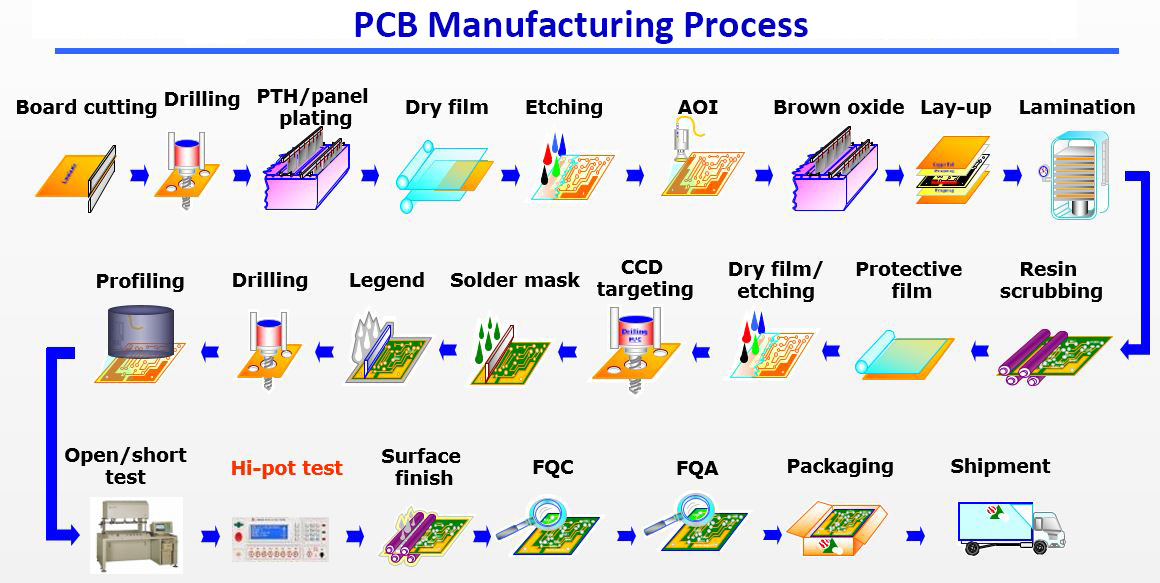
A Step-by-Step Guide To PCB Manufacturing Process
 www.nextpcb.com
A Step-by-Step Guide to PCB Manufacturing Process
22 Steps To Summarize The Entire PCB Design Process - IBE Electronics
 www.pcbaaa.com
22 steps to summarize the entire PCB design process - IBE Electronics
22 Steps To Summarize The Entire PCB Design Process – PCB HERO
 www.pcb-hero.com
22 steps to summarize the entire PCB design process – PCB HERO
PCB Process Flow Chart | Www.homillux.com
 www.homillux.com
PCB Process Flow Chart | www.homillux.com
Basic Steps To Design A PCB Layout – PCB HERO
 www.pcb-hero.com
Basic Steps to Design a PCB Layout – PCB HERO
A step-by-step guide to pcb manufacturing process. 22 steps to summarize the entire pcb design process – pcb hero. How to use a modular approach to simplify your pcb design process